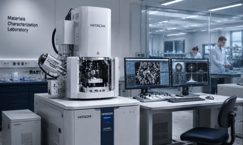
Hitachi scanning electron microscope (SEM) is a high-precision surface analysis and micro-characterization instrument independently developed by Hitachi High-Tech. Represented by mainstream models including SU3800, SU3900, SU7000 and SU8600, it features high resolution, low damage imaging, intelligent detection and strong environmental adaptability. Different from traditional optical microscopes, Hitachi SEM uses focused electron beams to scan sample surfaces and generates microscopic morphology, structural and component information through signal feedback. It has become indispensable core equipment in material science, industrial manufacturing, electronic semiconductor industry and scientific research laboratories. This article systematically elaborates the complete structural composition and detailed application scope of Hitachi SEM, providing technical reference for instrument application and industry research.
The complete structural system of Hitachi scanning electron microscope is mainly divided into four core modules: electron optical column, vacuum system, sample stage and chamber assembly, and signal detection and imaging system, with supporting intelligent control and cooling auxiliary systems. Each module cooperates precisely to ensure high stability and high precision of electron beam scanning and signal acquisition.
The electron optical column is the core component that determines imaging resolution, mainly including electron emitter, acceleration lens, focusing lens, scanning coil and aperture diaphragm. Most high-end Hitachi SEMs adopt Schottky field emission electron sources, which can produce high-brightness, high-stability and fine-diameter electron beams. Compared with traditional tungsten filament electron sources, it achieves lower imaging noise and higher microscopic resolution, realizing nano-scale ultra-fine structure observation. The multi-stage lens group precisely focuses the electron beam, while the scanning coil controls the electron beam to scan the sample surface in an orderly manner, completing regional microscopic imaging.
The vacuum system is a key guarantee for the normal operation of SEM. Hitachi SEM is equipped with a composite vacuum system composed of mechanical pump and molecular pump, which can quickly evacuate the electron column and sample chamber to high vacuum environment. It effectively prevents electron beam deflection and energy loss caused by air molecule collision, and avoids sample surface contamination and oxidation during observation. Some improved models support low-vacuum imaging mode, enabling direct observation of non-conductive, wet and porous samples without metal spraying pretreatment, greatly expanding sample adaptability.
The sample chamber and precision stage system are optimized for diverse experimental scenarios. Hitachi SEM features a large-capacity sample chamber and a high-precision multi-dimensional mobile stage, supporting the placement and observation of large-size, heavy-load samples. The stage can realize precise displacement, rotation and tilting adjustment, meeting multi-angle and large-area scanning imaging requirements. The chamber is reserved with multiple expansion interfaces, which can be externally connected with EDS, EBSD and other component analysis accessories to synchronously complete morphological observation and elemental composition detection.
The signal detection and imaging system consists of secondary electron detector, backscattered electron detector and intelligent image processing unit. The secondary electron detector is mainly used to capture sample surface morphology information with high stereoscopic effect, while the backscattered electron detector identifies material composition differences and impurity distribution according to atomic number contrast. The multi-channel signal synchronous acquisition technology of Hitachi SEM can superimpose and display multiple imaging signals in real time, realizing complementary analysis of morphology and components.
Hitachi scanning electron microscopes are widely used in multiple industries and scientific research fields with excellent comprehensive performance. In the semiconductor and electronic industry, they are applied to surface defect detection, circuit microstructure observation, wafer coating uniformity analysis and micro-nano component precision inspection, providing core data for chip manufacturing and quality control.
In material science research, Hitachi SEM is used for microstructure characterization of metal materials, new polymer materials, ceramic materials and nanomaterials. It can analyze material surface roughness, grain structure, fracture morphology and pore distribution, helping researchers verify material modification effects and optimize material formulas. In the chemical and environmental protection industry, it detects the microscopic morphology of pollutants, filter materials and adsorbents, supporting environmental treatment and chemical material research.
In industrial quality inspection and failure analysis, the instrument is widely used for product surface scratch detection, coating peeling analysis, material fracture failure and corrosion mechanism research, providing intuitive microscopic evidence for industrial product quality improvement and failure troubleshooting. In addition, it also plays an important role in biomedical observation, geological mineral microstructure analysis and forensic scientific research, realizing high-precision micro-characterization of diverse samples.
In summary, Hitachi scanning electron microscope has a sophisticated and modular structural design, with outstanding advantages in resolution, stability and sample adaptability. Its application scope covers scientific research, industrial manufacturing, quality detection and many other fields. With the support of perfect structural modules and intelligent imaging technology, it can efficiently complete microscopic morphology observation and material component analysis, providing reliable technical support for micro-scale scientific research and industrial precision production.